The project as a whole was really split into two major parts with a minor part at the very end. The first two main parts are the automation calculations and the BRAM storage for VGA display, and the third and final part was audio analysis.
In terms of the first part, the calculation itself, the program was implemented as a simple finite state machine with only a few sets of registers needed to influence those states. At first, the easiest way that it seemed to implement the calculations of each generation was to take a software implementation that we created and try to convert that calculation into a hardware version of that same calculation. This approach, while it gave the basic template for future solutions, didn’t fare too well once it came to actually implementing each cell value in the hardware design.
In software, we implemented design as two 1D arrays and a final 2D array to hold all of the final values. While this made sense while writing in software because all that was needed was a few nested for loops which made the code very compact, loops do not translate well into hardware. This design in hardware yielded latch and net driver errors for almost every register besides state and initial registers.
From there, the next approach was to have two maximum sized 1D arrays to hold each cell that would constantly read from each other in a state machine and alternatively write to BRAM until a maximum address value was reached. This design, while it made more sense after using a state machine to implement the previous design’s loops, still yielded driver errors and timing between the two arrays and BRAM quickly became a nightmare. This seemed like it would be the best design in terms of hardware usage and parallel computing because it used a minimum amount of registers to hold cells, and while one array was writing to BRAM, the other array could theoretically start reading from that same array to recalculate itself.
The final design for the calculations was a bit different from that best-case scenario design though. Because we couldn’t resolve the driver errors between the two 1D arrays, we created a single 2D array that held generation 0 in its first row, and computed off of previous rows to compute new generations. To improve timing with the BRAM as well, every generation is calculated in a state until a new “write” state is moved to. An FSM for how each cell was calculated is shown below 1.
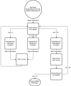
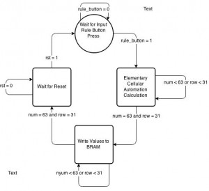
In this final design, the FSM designated as figure 1 is an FSM for the block in figure 2 labeled as “Elementary Cellular Automation”. In every scenario a rest state was created to allow a user to select a new automation if need be, but once the audio analysis begins reprogramming is needed if a new automation is to be selected. A final design FSM for the calculations is shown below 2.
As the cellular data was being loaded into the BRAM through Port A, the VGA display module was reading the data via Port B and analyzing it to be displayed on the external monitor through the VGA cable. The display module would iterate through each pixel on the screen by row, and if it was within the bounds of the blue border, output a blue pixel value. Each of the 2048 cells is represented by 16×16 pixels, and each pixel would calculate the BRAM address of which cell to read using addition, subtraction, and shifting. The VGA output requires a 75 MHz clock, so our top module creates this clock using phase shifting. This slower clock (from our board’s 100 MHz clock) is used to drive Port B of the original BRAM as well as the VGA display module, the second BRAM, and the audio component.
When the user presses the rotate button, a case statement replaces the address bus in Port B from the VGA display module input to the load module input. The load module takes the middle 16 columns of the represented cell data and loads it into a smaller BRAM via Port A. The VGA display then reads this data in an order that rotates the 16 columns by 90 degrees counter-clockwise by switching the row and column calculations.
When the user presses the play audio button, a case statement replaces the address bus in Port A of the smaller BRAM from the load module to the audio generation module. By using both ports of the smaller BRAM, we are able to output data from different addresses at the same time to both the audio generator and the VGA generator. The audio generator reads the first 16 cells of the BRAM (or the first column of the rotated display) and analyzes it to determine what note to play. Each column on the rotated screen represents a unit of time, and by using counters for each of the four channels, up to four different notes can be played at once by flipping the output pin high or low, creating a square wave.